Microelectronic Circuits
— HimanishLec 1 #
- Op Amp is the closest we can get to Ideal Amplifier
Lec 2 #
Superposition Theorem #
- used when there are multiple independent sources
- For each independent source, form a subckt with all other independent srcs set to zero. All voltage sources are shorted, all current sources are open.
- Find the response to that independent source acting alone for each subckt
- Total response is sum of individual responses.
Lec 3 #
Capacitor #
\[I = C \frac{dV}{dt}\] \[X_c = \frac{1}{j\omega C}\]
- At dc, \(\omega = 0\), open ckt
- At high freq ac, \(\omega \approx \infty\), short ckt
Inductor #
\[V = L \frac{dI}{dt}\] \[X_L = j\omega L\]
- At dc, \(\omega = 0\), short ckt
- At high freq ac, \(\omega \approx \infty\), open ckt
Amplifiers #
- \(v_i \sim \mu V\), \(v_o \sim mV\)
Linear Amplifier #
\[v_o (t) = Av_i(t)\]
- A: a constant independent of \(\omega\)
- If \(v_i = a \sin \omega t\), then \(v_o = Aa \sin(\omega t + \phi)\), only amplitude changes. Don’t worry about phase in this class. Either in-phase or out of phase.
- Non-linear amp: \(v_o(t) = f(v_i(t))\)
Gain #
\[A_p = \frac{v_oi_o}{v_ii_i} = A_VA_I\]
Decibels #
- V-Gain (dB) = \(20 \log_{10} |A_v|\) dB
- I-Gain (dB) = \(20 \log_{10} |A_I|\) dB
- Power Gain (dB) = \(10 \log_{10} |A_p|\) dB
Amp Power Supply #
\[P_{DC} = V_{CC}I_{CC}+V_{EE}+I_{EE} \] \[\underbrace{P_{DC}}_{\text{Power from supply}} + \underbrace{P_I}_{\text{i/p power in the signal}} = P_{\text{load}} + P_{\text{diss}} \] \[\eta = \frac{P_L}{P_{DC}}, \ P_I \ll P_{DC}\]
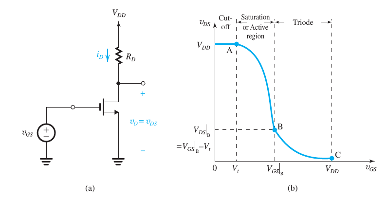
Amplifier Saturation #
- Linear amplification happens only over a range of inputs. Outside this range, no amplification occurs, distortion may happen.
- Output voltage is limited to \(\{L_-,L_+\}\) so \[\frac{L_-}{A_v} \le v_i \le \frac{L_+}{A_v}\]
Lec 4 #
Naming Convention #
- DC: Capital letters, \(V_O, I_C\)
- AC: Lowercase, \(v_c, i_c\)
- Total current = DC + AC so \(i_C(t) = I_C+i_c(t)\).
- DC power supplies: \(V_{CC} , V_{DD}\).
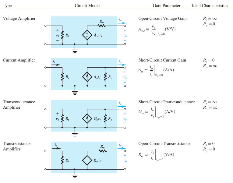
Voltage Amplifier Model #
- \(v_i, v_o, A_v\)
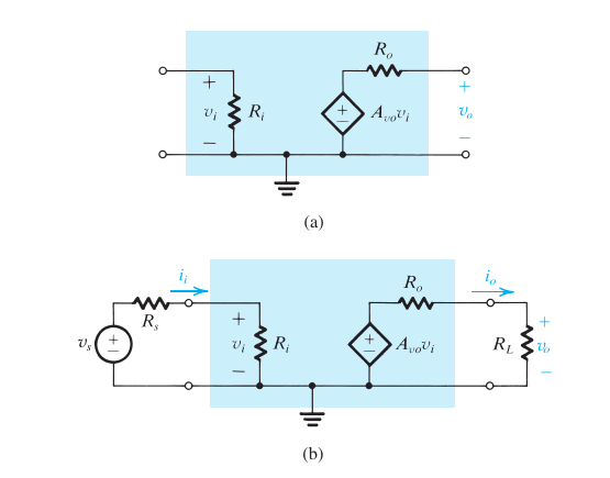
- For ideal volt amp, \(R_{in} = \infty\), \(R_{out} = R_o = 0\)
- only a fraction of the source signal v s actually reaches the input terminals of the amplifier
- Thus, net gain < \(A_v\)
Amplifier with Load and Signal #
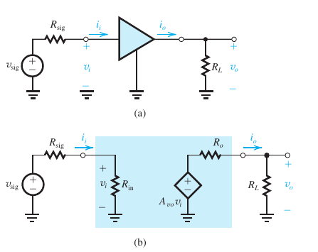
Measurement #
- Open ckt voltage gain
- \[R_{in} = \frac{v_i}{i_{in}}\]
- \[R_o = v_o/i_o\]
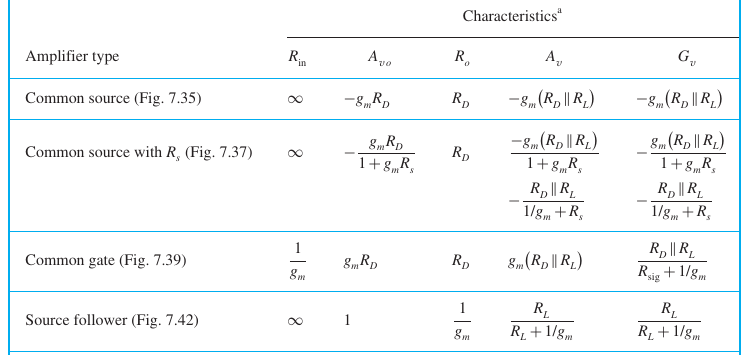
Amplifier Types #
Cascade Amps #
Lec 5 #
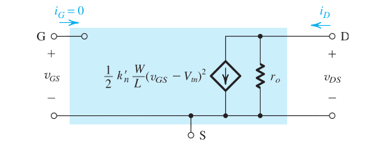
MOSFET #
- Neglect body effect, was only an issue in older technologies.
- Gate current is zero, i.e. \(I_G = 0\). Only gate voltage matters.
- Threshold voltage is at which inversion occurs, i.e. drain becomes source
MOSFET Params #
- Design Params: W, L (\(\frac{W}{L}\)); Less flexibility to change L
- Process Params: \( V_{DD}, V_T, T_{ox}, N_{sub} \)
- Process transconductance parameter \(k_n’ = \mu_nC_{ox}\)
- MOSFET transconductance parameter \(k_n = \mu_nC_{ox}(W/L)\)
Lec 6 #
Channel Length Modulation #
- At some point in saturation, in pinchoff: as we increase \(V_D\), \(\Delta L\) increases which reduces effective channel length from \(L \text{ to } L-\Delta L\)
- We can model this non-ideality using the channel length modulation factor \(\lambda \propto \Delta L/ L\): \[I_{DS} = \frac{1}{2}\mu_{neff}C_{ox}\frac{W}{L}(V_{GS}-V_T)^2(1+\lambda V_{DS})\]
- \(\frac{\partial I_{DS}}{\partial V_{DS}} = \lambda I_{DSAT}\)
- Thus, resistance \[r_0 = \frac{1}{\lambda I_{DSAT}}\]
- In terms of Early effect: \(\lambda = \frac{1}{V_A}\) where \(V_A\) is the Early voltage.
- \[V_A = V_A’ \cdot L\]
Transconductance #
\[g_m = \frac{\partial I_{DS}}{\partial V_{GS}}\] \[g_m = k_n’(W/L)\overbrace{(V_{GS}-V_T)}^{overdrive}\] \[g_m = \sqrt{2\mu_nC_{ox}(W/L)I_D} \] \[g_m = \frac{2I_D}{V_{GS}-V_T}\]
Body effect #
- When source and body are not tied together
- Not used in this class
Long Signal Models #
Lec 7 #
Small Signal Model #
- \(I_{ds} = I_{DS}+i_{ds}\): Amplitude of \(i_{ds}\) is very smol.
- Small signal parameters depend on the biasing point we choose
Linearisation of I-V characters around a bias point #
- At a bias point: \(I_{DS}, V_{GS}, V_{DS}\)
- Since \(I_{DS} = f(V_{GS}, V_{DS}) \), and we think of the small signal \(i_{ds}\) as a variation in the dc signal, we can say
\[i_{ds} = \Delta I_{DS} = \frac{\partial f}{\partial V_{GS}}v_{gs}+\frac{\partial f}{\partial V_{DS}}v_{ds}\] \[i_{ds} = \frac{\partial I_{DS}}{\partial V_{GS}}v_{gs}+\frac{\partial I_{DS}}{\partial V_{DS}}v_{ds}\]
- Assume an NMOS in saturation: \[I_{DS} = \frac{1}{2}k_n(V_{GS}-V_T)^2(1+\lambda V_{DS})\]
\[i_{ds} = \frac{\partial I_{DS}}{\partial V_{GS}}v_{gs}+\frac{\partial I_{DS}}{\partial V_{DS}}v_{ds}\]
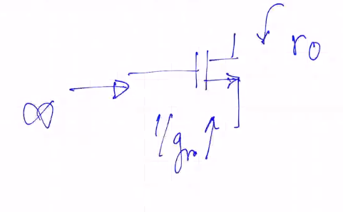
\[i_{ds} = g_mv_{gs}+\frac{v_{ds}}{r_0} \text{ where } \ r_0 = \frac{1}{\lambda I_D}\]
\(i_{ds} = g_mv_{gs}\) when no channel-length modulation
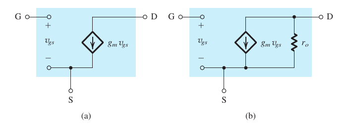 (a): No channel length modulation
(b): With channel length modulation
(a): No channel length modulation
(b): With channel length modulation
Lec 8 #
Transistor Amplifier #
 \[A = \frac{v_o}{v_i} = -g_mR_D\]
- Negative gain implies inverting amplifier, i.e. \(180^\circ\) phase between input and output.
- When channel-length modulation is accounted for:
\[A_v = \frac{v_o}{v_i} = -g_m(r_0||R_D)\]
CMOS Amplifier #
- Common Source (CS)
- Common Gate (CG)
- Common Drain (CD) or Source Follower
CS Amplifier #
\[A_v = -\sqrt{2k_n’(W/L)I_D}R_D\]
- For high gain, we need to increase \(I_D, R_D\) but that makes it harder to keep \(M_1\) in saturation
Lec 9 #
CS Amp #
- For high gain, increase \(R_D\) till infinity so that it becomes an ideal current source
- So \(A_v = -g_mr_o\), \(R_{on} = \infty\), \(R_{out} = r_o\)
- For an ideal MOS, \(r_o = \infty\) so gain is infinite
- We can get an ideal current source by using another MOS in saturation
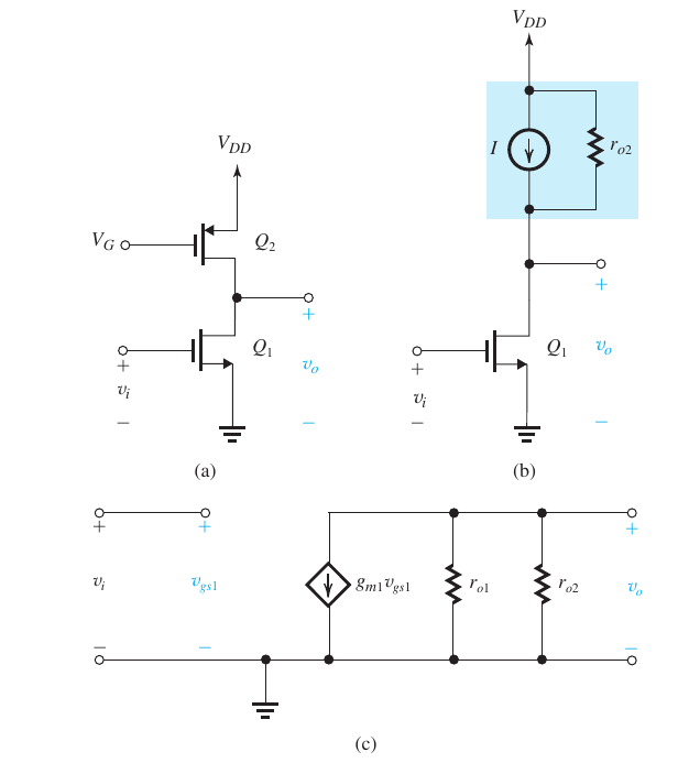
- \[A_v = -g_{m1}(r_{o1}||r_{o2})\]
- As \(Q_1\) is converting the input voltage to output current, it is doing the transconductance
Lec 10 #
CS Stage with Source Resistance (Degeneration) #
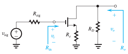
- We use \(R_S\) to control the magnitude of the signal \(v_{gs}\) and thereby ensure that \(v_{gs}\) does not become too large and cause unacceptably high nonlinear distortion.
- But \(R_S\) will bring stability to gain at the cost of reducing it.
- \[v_{gs} = \frac{v_{in}}{1+g_mR_S}\]
- \( v_o = - g_mv_{gs}R_D\)
- \[A_v = \frac{v_o}{v_{in}} = \frac{-g_mR_D}{1+g_mR_S} = - \frac{R_D}{1/g_m + R_S} = -G_MR_D\]
- If a load resistance \(R_L\) is connected at the output, replace \(R_D\) by \(R_D || R_L\)
- The factor \((1+g_mR_s)\) is the amount of negative feedback introduced by \(R_s\)
- Voltage gain from gate to drain = \(- \frac{\text{Total resistance in drain}}{\text{Total resistance in source}}\)
- \[R_{out} = r_o + (1+g_mr_o)R_S\]
- \(R_{in} = \infty\)
Lec 11 #
Coupling Capacitor #
- In DC Analysis, treated as open
- For small signal ac analysis, shorted
- So, it only lets the ac component of the signal through.
- For large capacitance, area of cap needs to be high which is not possible in integrated ckts, so we have to use differential amps
Lec 12 #
Common Gate Amplifier #
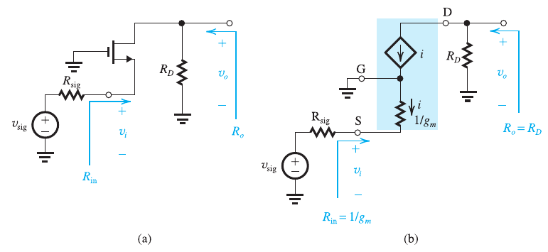
- \(R_{in} = \frac{1}{g_m}\)
- \(A_{v} = g_mR_D\)
- \(R_{o} = R_D\)
- The CS configuration suffers from a limitation on its high-frequency response
- Combining the CS amp with a CG amp can extend the bandwidth considerably
Lec 13 #
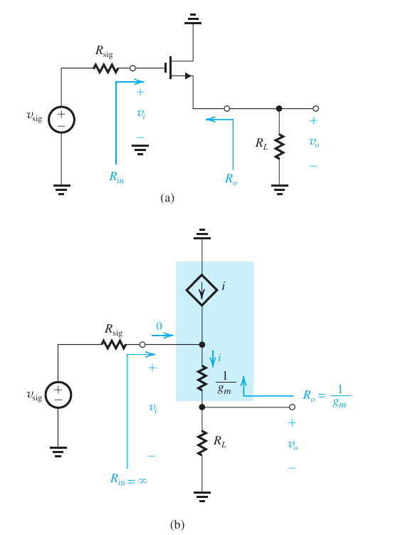
Source Follower (Common-Drain) #
-
\[A_v = \frac{g_m(r_o||R_L)}{1+g_m(r_o||R_L)} = \frac{r_o||R_L}{\frac{1}{g_m}+(r_o||R_L)} \approx 1\]
- Thus, used as a voltage buffer.
-
\(R_{in} = \infty\)
-
\(R_{out} = \frac{1}{g_m}\)
-
\(R_L, (W/L), V_{GS}(\text{or } V_{ov})\) are the parameters to calculate for designing a circuit
Problems with Resistors #
- Occupy too much space on the SoC
- Generate heat which heats up all the components around it and \(n_i^2 \propto e^{-1/T}\)
- We test the design at high temperatures to check for the worst case
- Speed up transistor aging and \(I_D\) starts dropping
Thus, other than discrete designs, resistors aren’t used for biasing. We use current source biasing in IC designs.
Lec 14 #
Cascode Amplifier #
- Cascoding: using a CG xtor to provide current buffering for the output of a CS/CE xtor
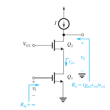
- \(R_{in} = \infty\) (gate)
- Comparing with a source-degenerated CS amp, \(R_s = r_{o1}\) so \[R_o = (g_{m2}r_{o2}) \ r_{o1}\]
- \[A_v = -g_{m1}R_o = -(g_{m1}r_{o1})(g_{m2}r_{o2})\]
Effective Transconductance #
\(A_v = - G_m R_{out}\)
- To calculate the effective transconductance \(G_m\), ground the output and measure \(i_{out}\) as a function of \(v_{in}\)
\[G_m = \frac{i_{out}}{v_{in}}\]
- To calculate \(R_{out}\), short the input voltage and measure \(v_{out}\) as a function of \(i_{out}\) \[R_{out} = \frac{v_{out}}{i_{out}}\]
Cascode Current Source #
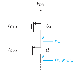
- For a gain of \(A_0^2\), the load \(R_L\) must be the same order as \(R_o\) of the cascode amplifier
- \(Q_3\) raises the output resistance of the current source \(Q_4\)
Cascode Amp with Cascode i-Src Load #
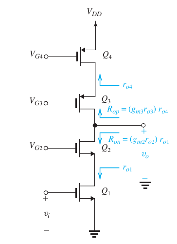 \[A_v = -g_{m1}[R_{on} || R_{op}]\]
- If all transistors are identical \[A_v = -\frac{1}{2}(g_mr_o)^2\]
Lec 15 #
Current Mirrors #
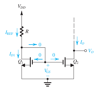
- \(I_{REF} = I_{D1} = \frac{1}{2}k_n’(W/L)_1(V_{GS}-V_{Tn})^2\)
- \(I_O = I_{D2} = \frac{1}{2}k_n’(W/L)_2(V_{GS}-V_{Tn})^2\)
- \[\frac{I_O}{I_{REF}} = \frac{(W/L)_2}{(W/L)_1}\]
- In case of identical xtors, the circuit becomes a current mirror
Effect of \(V_O\) on \(I_O\) #
To ensure \(M_2\) is saturated, \(V_O \ge V_{GS}- V_{Tn}\) \(V_O \ge V_{OV}\)
Channel Length Modulation #
\(R_O := \frac{\Delta V_O}{\Delta I_O} = r_{o2} = \frac{V_{A2}}{I_O}\) \[I_O = \frac{(W/L)_2}{(W/L)_1}I_{REF}(1+\frac{V_O-V_{GS}}{V_{A2}}\]
Current Steering #
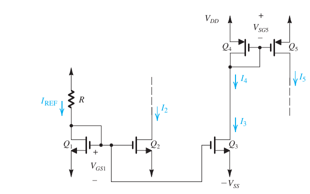
- Xtors \(M_1, M_2, M_3\) form a two-output current mirror.
\[I_2 = I_{REF}\frac{(W/L)_2}{(W/L)_1}\] \[I_3 = I_{REF}\frac{(W/L)_3}{(W/L)_1}\]
- \(I_3\) is fed to the input of a i-mirror formed by pMOS xtors \(M_4, M_5\)
\[I_5 = I_4 \frac{(W/L)_5}{(W/L)_4}\] \[V_{D5} \le V_{DD} - |V_{OV5}|\]
- While \(M_2\) pulls its current \(I_2\) from a circuit (not shown), \(M_5\) pushes its current \(I_5\) into a circuit (not shown). Thus \(M_5\) is appropriately called a current source, whereas \(M_2\) should more properly be called a current sink. In an IC, both current sources and current sinks are usually needed.
Small Signal of Current Mirror #
\[A_{i} = \frac{g_{m2}}{g_{m1}} = \frac{(W/L)_2}{(W/L)_1}\]
Lec 16 (Mane Arc Begins) #
\[A_v = \frac{\text{Output Resistance}}{\text{Resistance seen through source}}\]
MOS Differential Pair #
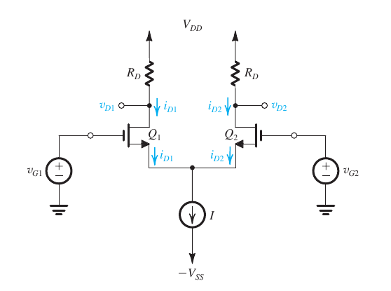 Two matched xtors whose sources are joined together and biased by a current source.
Common-Mode Input Voltage #
- When equal voltages are applied at gate, i.e. \(v_{G1} = v_{G2} = V_{CM}\)
- As xtors are matched, \(i_{D1} = i_{D2} = I/2\)
- \[\frac{I}{2} = \frac{1}{2}k_n’(W/L)V_{OV}^2\]
- \[V_{OV}= \sqrt{\frac{I}{k_n’(W/L)}}\]
- \[v_{D1} = v_{D2} = V_{DD} - (I/2)R_D\]
- Thus, diff in output voltage will be zero, i.e. differential pair does not respond to common-mode inputs.
- Since both xtors must remain in saturation, there would be a range over which the diff-pair operates properly,
- \[V_{CM_{max}} = min(V_{DD}, V_{DD} - (I_{SS}/2)R_D + V_T)\]
- \[V_{CM_{min}} = -V_{SS} + V_{CS} + V_T + V_{OV}\]
- \[V_{CM_{min}} = V_{ISS} + V_{GS_1} = V_{ISS} + V_{OV} + V_T \]
Differential Input Voltage #
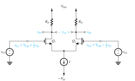
- For all the current \(I_{SS}\) to flow through \(M_1\), the current through \(M_2\) must be zero which happens at cutoff, i.e. \(V_{GS_2} = V_T\)
- \(V_{in_1}-V_{GS_1}+V_{GS_2}-V_{in_2}=0\)
- \(2V_{in_1}= V_{GS_1}- V_{GS_2}\)
- \(2V_{in_1}= V_{GS_1}- V_T = V_{OV_1}\)
- Thus, \(v_{id_{max}} = \sqrt{2}V_{OV}\)
- Must be operated between the range:
\[-\sqrt{2}V_{OV} \le v_{id} \le \sqrt{2}V_{OV}\]
\[\\ \text{offline modo hiatus} \\ \]
Frequency Response #
- Thus far, we have been assuming that our amplifiers are operating in the middle-frequency band or midband, where the gain is almost constant.
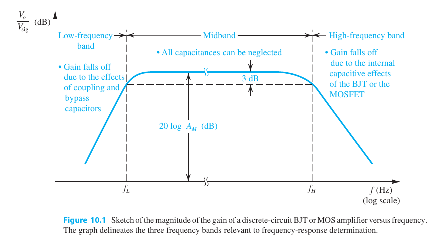
- However, at lower frequencies, the magnitude of the amplifier gain falls off.
- Coupling and bypass caps no longer have low impedances
- \(r_o\) is neglected, as has a negligible effect in discrete-circuit amps
Bandwidth #
- \(BW = f_H - f_L\) [discrete circuit amps]
- \(BW = f_H \) [integrated circuit amps]
Here, \(f_H\) is the upper end of the midband.
Gain-Bandwidth Product #
\[GB = |A_M|\text{BW}\]
Unity-Gain Frequency #
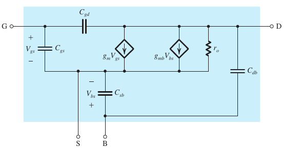
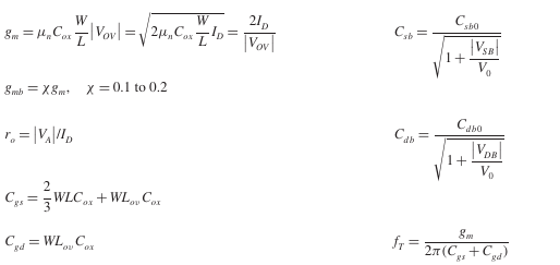
\[f_T = \frac{g_m}{2\pi(C_{gs}+C_{gd})}\]
High Frequency Model #
Miller’s Theorem #
Miller Multiplication #
\[C_{in} = C_{gs} + (1 - A_v)C_{gd}\]