Electronic Devices
— HimanishImportant Values (Si) #
\[n_i = 1.5e10 /cc\] \[N_c = 2.8e19 /cc\] \[N_v = 1.04e19 /cc\] \[\epsilon_r = 11.9\]
Overview #
We want to answer two questions.
- How many charge carriers are there?
- E/k band diagram \(\rightarrow\)Effective Mass
- Density of states
- Fermi-Dirac Statistics
- Where are they and how are they moving?
- Carrier Drift \(\rightarrow\) Ohm’s Law
- Carrier Diffusion
- Generation and Recombination
- Continuity Equation
3D Crystals #
| Property | Simple (sc) | Body centered (bcc) | Face centered (fcc) |
|---|---|---|---|
| Number of atoms | \(8\cdot\frac{1}{8} = 1\) | \(8\cdot \frac{1}{8} + 1 = 2 \) | \(8 \cdot \frac{1}{8} + 6 \cdot \frac{1}{2} = 4 \) |
| Nearest neighbour distance | \(a\) | \(\frac{\sqrt{3}a}{2}\) | \(\frac{a}{\sqrt{2}}\) |
Miller Indices #
Three integers used to describe a plane.
How to find #
- Find intercepts of plane with crystal axes expressed in terms on basis vectors, e.g. 2 a, 4 b, 1 c
- Take reciprocals of these numbers: \(\frac{1}{2} \frac{1}{4} 1\)
- Reduce to integers and label as (hkl):
(2 1 4)
Notations #
- If an intercept occurs on the negative branch of an axis, the minus sign is placed above the Miller index for convenience, such as \((h \overline{k} l)\).
- Many planes in a lattice are equivalent; that is, a plane with given Miller indices can be shifted about in the lattice simply by choice of the position and orientation of the unit cell. Such equivalent planes are denoted using
{}instead of(). For example, the six equivalent faces of a cubic lattice are collectively designated as{100}. []brackets are used for direction indices, e.g. the body diagonal of a cubic lattice can be designated [1 1 1].<>is used for equivalent direction indices, e.g. all crystal axes[100], [010], [001]are denoted<100>.
Useful relations #
- The shortest distance d between two adjacent planes labeled (hkl) is given in terms of the lattice constant a as: \[ d = \frac{a}{\sqrt{h^2 + k^2 + l^2}} \]
- The angle u between two different Miller index directions is given by \(\cos \theta =\frac{h_{1} h_{2}+k_{1} k_{2}+l_{1} l_{2}}{(h_{1}^{2}+k_{1}^{2}+l_{1}^{2})^{1 / 2}(h_{2}^{2}+k_{2}^{2}+l_{2}^{2})^{1 / 2}}\)
- The direction [\(hkl\)] is perpendicular to the plane (\(hkl\))
Atomic Densities #
\(1 Å = 10^{-8} cm\)
- \[\text{Volume density} =\frac{\text{\# atoms in cell}}{V_{cell}} \]
- \[\text{Areal density} =\frac{\text{\# atoms in cell}}{SA_{cell}} \]
Diamond Lattice #
- The diamond structure can be thought of as an fcc lattice with an extra atom placed at
a/4 + b/4 + c/4from each of the fcc atoms. Thus, the original fcc has associated with it a second interpenetrating fcc displaced by1/4 , 1/4 , 1/4. - Si, Ge form diamond like lattice
- Si unit cell has 8 edge (red) atoms, 6 (green) face atoms and three atoms at the centers of smaller cubes forming a tetrahedral bonding. A total of \(N = \frac{1}{8} \cdot 8 + \frac{1}{2} \cdot 6 + 4 = 8 \) atoms per unit cell
Energy Bands and Charge Carriers #
- The upper band (called the conduction band) contains 4N states, as does the lower (valence) band. Thus, apart from the low-lying and tightly bound “core” levels, the silicon crystal has two bands of available energy levels separated by an energy gap \(E_g\) wide, which contains no allowed energy levels for electrons to occupy. This gap is sometimes called a “forbidden band,” since in a perfect crystal it contains no electron energy states.
Electrons and holes #
- Electrons (
n) in conduction band and holes (p) in valence band contribute to current. - \(n \propto T\)
- Holes are generally heavier than electrons (Effective mass)
Fermi-Dirac Statistics #
- Fundamental particles in nature have either integer spin and are called bosons (e.g. photons), or half-integer spin and are known as fermions (e.g. electrons).
- Fermions follow Fermi-Dirac statistics, thus probability of finding electron at any energy state E is \[f(E) = \frac{1}{1+\text{exp}(\frac{E-E_F}{kT})} \] where \(k = 8.62 e\text{-}5 \quad \text{eV/K} = 1.38 \) J/K and \(kT = (\frac{T}{300})25.9\) meV
- Probability of finding a hole at energy \( E = 1 - f(E)\)
- In a quantum mechanical system with many energy levels, the density of energy states per unit volume per unit energy is given by \[g(E)=\frac{4 \pi(2 m)^{3 / 2}}{h^{3}} \sqrt{E}\]
- The density of states in the conduction band \(E > E_c\)is given by \[g_{c}(E)=\frac{4 \pi\left(2 m_{n}^{*}\right)^{3 / 2}}{h^{3}} \sqrt{E-E_{c}}\]
- The density of states in the conduction band \(E < E_v\)is given by \[g_{v}(E)=\frac{4 \pi\left(2 m_{p}^{*}\right)^{3 / 2}}{h^{3}} \sqrt{E_{v}-E}\]
- The number of occupied states between energies E1 and E2 is given by \[ N = \int_{E_1}^{E_2} g(E)f(E)dE \]
* (Boltzmann approximation) For energies much greater than the Fermi energy (\(E-E_F \geq 3\) kT), the distribution function can be approximated as \( f(E) = \text{exp}(-\frac{E-E_F}{kT})\), thus
- \[ \boxed{n = N_c \text{ exp}\left(-\frac{E_c-E_F}{kT}\right)}\]\( (\int_{E_c}^{\infty} g_C(E)f(E)dE)\)
- \[ \boxed{p = N_v\text{ exp}\left(-\frac{E_F-E_v}{kT}\right)}\] \((\int_{-\infty}^{E_v} g_v(E)f(E)dE) \)
Semiconductor at thermal equilibrium #
- No discontinuity or gradient can arise in the equilibrium Fermi level \(E_F\).
- Consider two materials in intimate contact such that electrons can move between the two.
- Rate of transfer of electrons from material 1 to 2 \(\propto\) (Filled states in 1) (Empty states in 2)
- \(R_{1 \rightarrow 2} \propto (N_1f_1(E)) (N_2[1-f_2(E)]) \)
- \(R_{2 \rightarrow 1} \propto (N_2f_2(E)) (N_1[1-f_1(E)]) \)
- At equilibrium, these two are equal. Rearranging terms, we get\(f_1(E) = f_2(E)\)
- Thus, \(\frac{dE}{dx} = 0\)
Intrinsic semiconductors #
- \(n = p = n_i\), thus\[ N_c \text{ exp}\left(-\frac{E_c-E_F}{kT}\right) = N_v\text{ exp}\left(-\frac{E_F-E_v}{kT}\right)\] \[\therefore E_i := E_{F (intrinsic)} = \frac{E_c + E_v}{2} + \frac{kT}{2}\log \frac{N_v}{N_c} \] (close to midgap in Si, Ge)
- Law of mass action: \(np = n_i^2 \text{(valid at equilibrium)}\)
- \[ n_i^2 = N_cN_v \text{ exp}\left(-\frac{E_c- E_v}{kT}\right)\] \[ n_i = \sqrt{N_cN_v}\text{ exp}\left(\frac{-E_g}{2kT}\right)\]
- As \(T \uparrow, n_i \uparrow \uparrow\)
Drift of Carriers in Fields #
Drift Velocity and Mobility #
\(v_d = \begin{cases} \mu E & E < E_c \text{ [low field]}\\ v_{sat} & E \geq E_c \text{ [high field]} \end{cases} \) \(\text{where } \mu: \text{mobility } = \frac{q\tau}{m^*}\)
- \[ \frac{1}{\mu_{eff}} = \sum_k \frac{1}{\mu_k}\]
Resistivity #
\[ \frac{V}{I} = R = \frac{\rho l}{A} \text{ where } \rho = \frac{1}{q(n\mu_n+p\mu_p)}\]
Hall Effect #
\[V_H = \mathcal{E}_y\cdot w = \frac{I_x\mathcal{B}_z}{qn_0}\cdot w = \mu_n\mathcal{E}_x\mathcal{B}_zw \]
Extrinsic semiconductors #
| Substitute one Si atom with B | Substitute one Si atom with P |
|---|---|
| B: p-type dopant | P, As: n-type dopants |
| # holes = # B atoms, \(p = N_A\) | # electrons = # P atoms, \(n = N_D\) |
| hole rich \(\rightarrow\) p-type semiconductor | electron rich \(\rightarrow\) n-type semiconductor |
- When \(N_D\) or \(N_A\) is of the order of \(n_i\), use \[ \boxed{p + N_D=n+N_A}\]
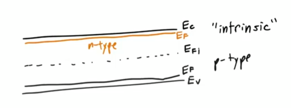
N-type #
- \[ E_c - E_F = kT \log \frac{N_c}{n} = kT \log \frac{N_c}{n}\]
- \[ E_F - E_i = kT \log \frac{N_D}{n_i} \] Thus Fermi level is above intrinsic level (midgap) in a n-type
- \[\rho \approx \frac{1}{q\mu_nN_D }\]
P-type #
- \[\rho = \frac{1}{q\mu_p(N_A)N_A }\]
- \[p = n_i\text{ exp}\left(\frac{E_i-E_F}{kT}\right) \]
Excess Carriers in Semiconductors #
Excess carriers are different from doping; in doping, the semiconductor stays in equilibrium, whereas creating excess carriers disturbs it.
Optical Absorption #
-
A photon with energy \(h\nu > E_g\) can be absorbed in a semiconductor to generate an
EHP. Less than that, and it passes through. -
\[ - \frac{dI}{dx} = \alpha I(x) \] \[\therefore I(x) = I_0e^{-\alpha(\lambda) x} \]
-
\[ I = Aqn_0\mu_nE\]
-
\( 1 \mu m = 10^{-4} cm\)
-
\( v_{d(sat)} = 10^7 cm/s\)
-
-
\[ t_{drift} = \frac{\Delta x}{v_d}\]
-
\[J = q[n\mu_n+p\mu_p]\mathcal{E} = \sigma E \]
\[\sigma = \begin{cases} \sigma_n & [n-type]\\ \sigma_p & [p-type] \end{cases} \]
- \[\mathcal{E} = \frac{V}{l}\]
Formal Analysis #
- As a system always tries to re-establish equilibrium, when light is impinged on a semiconductor, creating excess carriers i.e.\(np > n_i^2\), recombination rate R shoots up to go back home. [net recombination occurs: R > G]
- On the flip side, when carriers are extracted e.g. in a pn junction, thus making \(np < n_i^2\), G>R.
Carrier Lifetime and Photoconductivity #
- Low level injection: equal number of electrons and holes added, while it doesn’t make a difference to majority carrier, it is significant for minority carriers, thus \[\frac{\partial p}{\partial t} = -\frac{\Delta p}{\tau_p}[\text{n-type}]\] \[\frac{\partial n}{\partial t} = -\frac{\Delta n}{\tau_n} [\text{p-type}]\]
- Continuity Equation \[\boxed{\frac{\partial p}{\partial t} = G - R - \frac{1}{q}\frac{\partial J_p}{\partial x}}\]
\[\\delta n(t) = \Delta n e^{-t/\tau_n} \\ | \\ \tau_n = (\alpha_rp_0)^{-1}\]
- In general, \(\tau_n = \frac{1}{\alpha_r(n_0+p_0)}\)
- Excess carrier concentration in terms of optical generation rate\[\delta n = \delta p = g_{op}\tau_n\]
- \[\boxed{n = n_i \text{ exp}\left(\frac{F_n-E_i}{kT}\right)}\]
- \[\boxed{p = n_i \text{ exp}\left(\frac{E_i-F_p}{kT}\right)}\]
- \[\frac{D}{\mu}=\frac{kT}{q}\]
Diffusion of Carriers #
\[J_n (\text{diff.}) = qD_n \frac{dn}{dx}\] \[J_p (\text{diff.}) = -qD_p \frac{dp}{dx}\]
Junctions #
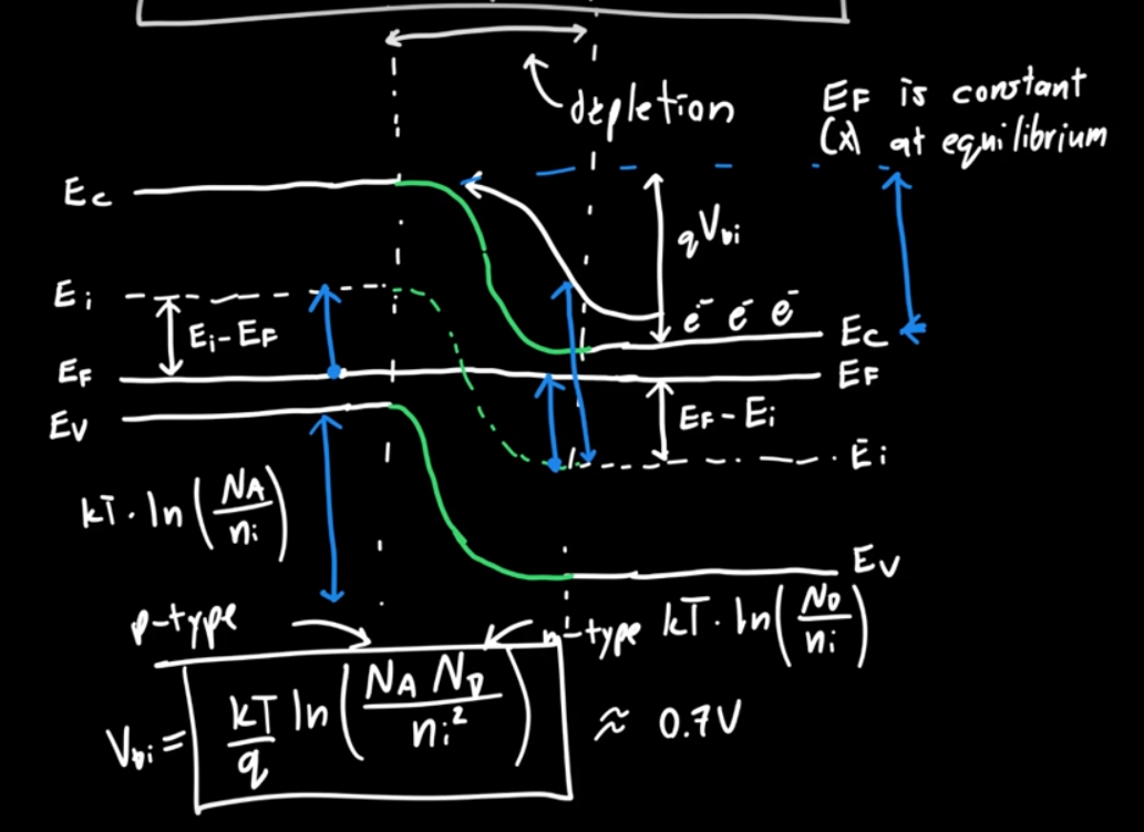
- If \(x_n, x_p \rightarrow\) depletion width of n-side and p-side respectively, then \[x_p \cdot N_A = x_n\cdot N_D\]
- Thus depletion width is higher on lightly doped side in pn junction
- \[\text{Depletion width } W = \frac{2\epsilon V_{bi}}{q}(\frac{1}{N_a}+\frac{1}{N_d})^{1/2}\]
- Built in potential\[V_{bi} = V_T \ln\left(\frac{N_AN_D}{n_i^2}\right)\]
- \[E_{max} = \frac{qN_A}{\epsilon_{Si}}x_p\]
PN Junction Diode #
- If we apply a voltage \(V_D\) across the PN junction, the built-in potential is reduced by this diode potential, so we can replace \(V_{bi}\) by \((V_{bi} - V_D)\) everywhere.
- Applying this voltage is like shining light on one side of semiconductor.
Relating carrier concentration on p-side and n-side #
\[p_{n0} = p_{p0}e^{-(V_{bi} - V_D)/V_T} \] \[ n_{p0} = n_{n0}e^{-(V_{bi}-V_D)/V_T}\]
Solving the Continuity Equation #
- Since \(\Delta p \ll p_0\) on the p-side and \(\Delta n \ll n_0\) on the n-side, we only need to solve the continuity equation for \(\Delta n\) on p-side and \(\Delta p\) on n-side. [Low-level injection (\(V_D \ll V_{bi}\))]
- We can neglect recombination in depletion region, and generation is small relative to injection from one side to another. Also, in steady state, carrier concentration becomes unchanging, thus we are left with \(\frac{1}{q}\frac{\partial J_P}{\partial x} = 0\), i.e.
- \(J_p\) and \(J_n\) are constant throughout depletion region and \(J = J_n + J_p\) is constant everywhere in the PN junction. The depletion region has no carriers, any entering will be swept across.
- \[\frac{\partial^2\Delta p}{\partial x^2} = \frac{\Delta p}{L_p^2}\] where \(L_p=\sqrt{D_p\tau_p}:\) diffusion length
\[\Delta p = A\exp{-\frac{x}{L_p}} + B\exp{\frac{x}{L_p}} \ \ \ [\text{B=0 unless short diode}] \]
- \[\Delta p(x) = p_{n0}(e^{V_D/V_T}-1)e^{-x/L_p}\]
- \[J_{n,sat} = \frac{qD_nn_{p0}}{L_n} = \frac{qn_i^2D_p}{L_pN_D}\] \[J_{p,sat} = \frac{qD_pp_{n0}}{L_p} = \frac{qn_i^2D_n}{L_nN_A}\] (Lightly doped side contributes to current)
\[J_{sat} = J_{n,sat} + J_{p,sat}\] \[\boxed{J(V) = J_{sat}(e^{V_D/V_T}-1)}\]
- \[\boxed{I_D = I_S(e^{V_A/V_T}-1)}\]
- \(I \approx I_Se^{V_D/V_T}\)Under forward bias when \(V > 3V_T\)
- \(I \approx -I_S\)Under reverse bias when \(|V| > 3V_T\)
- \(J_S \propto \exp(-E_g/T)\)
\[J \propto \exp\left(\frac{-(E_g-qV_A)}{kT}\right)\]
One-sided diode #
- \(P^+N\) junction is formed when \(N_a \gg N_d \). The depletion region extends mostly towards the n-side.
Equilibrium #
When a zero bias voltage is applied across the junction, the junction is in equilibrium. No ’net’ current flows across the junction. The drift and diffusion currents cancel each other \[J_{\text{p,diff}} = J_{\text{p,drift}} \ \ \ J_{\text{n,diff}} = J_{\text{n,drift}}\]
Forward Bias #
- Majorly diffusion current from p to n
Reverse Bias #
- When a negative bias voltage is applied across the junction, the equilibrium is disturbed. Assuming that the p and n regions have very low resistivity, most of the applied voltage drops across the depletion region.
- Thus the voltage across the junction opposes the diffusion current, the diffusion current is almost non-existant under the rever applied bias. Only drift current dominates.
Diffusion Capacitance and Resistance #
- A differential change in the reverse bias leads to a differential change in the charge. This can be seen as a capacitive effect:
\[C_{diff} = \frac{dQ}{dV} \frac{qAe^{V_0/V_T}}{2V_T}(L_nn_{p0}+L_pp_{n0}) \ \ \ [V_0: \text{bias voltage}\]
- Normally depletion capacitance (\(C_j\)) is defined per unit area (\(C_j = C/A\)) in pn junctions thus we have
\[C_j = \sqrt{\frac{q\epsilon}{2(\frac{1}{N_A} + \frac{1}{N_D})(V_{bi}-V_A)}} \text{(varicap)}\]
- \(C_j\) also depends on doping concentration profile. If \(N_D(x) = Gx^m\), \(C_{rb} \propto V_R^{-n}\), where \(n = \frac{1}{m+2}\)
- \[r_d = \frac{V_T}{I_D}\]
Short Base Diode #
- If length of n region \((\ell) \ll L_p\), Recombination rate = Zero as insufficient length available for holes to recombine
- Thus \(\frac{d^2\Delta p}{dx^2} = 0 \implies \Delta p = mx + c\)
- In the short side, replace recombination length by width, e.g. \(L_p\) by W.
- At the contact, no excess carriers are present as metal contact has infinite carriers that nullify them, i.e. full recombination.
Non-idealities #
- If \(V_A ~ 0.7 - 1 V\), the series resistance of p and n side kicks in and limits the current, i.e. current reaches saturation at high voltages. At small currents, contact resistance can be neglected.
- Recap: R > G if \(np > n_i^2\) else R < G.
Space Charge Generation-Recombination Current #
- Traps reduce idealities, causing \(I_{FB} \downarrow, I_{RB} \uparrow\)
- Consider diode in
RB. In ideal model, we only had \(J_0\). But now due to traps, \(np < n_i^2\) in the depletion region, causing net generation to realise equilibrium. Thus the actual RB current has an additional \(J_G\) term (\(\propto N_T, T\)), thus \(I_{RB}\uparrow\). - In
FB, more carriers, so net recombination, so \(J_{FB}’ = J_0 - J_R\), thus current decreases.
Breakdown #
- At \(E_{crit}\), breakdown occurs. \[E_{crit} = \frac{2(V_{bi}+V_R)}{W}\]
Zener Breakdown #
- Heavily doped diode
- Tunneling mechanism: Tunneling \(\propto \exp{(-W)}\) [depletion width matters]
- Less dependent on temperature
Avalanche Breakdown #
- Lightly doped diode
- One electron enters depletion region, uses the electric field energy to generate an EHP, which in turn produce their own EHPs, causing lot of current.
- Multiplicative factor M = \((1+P)^N\) where \(N = \lfloor W/\lambda \rfloor\)
- Holes bubble up to the top, electrons roll down the hill of band bending.
Switching in P-N junction #
- If we apply a sinusoidal voltage across the diode, it takes time for the diode to switch from forward to reverse bias as recombination of excess carriers is not instantaneous
- To increase the switching speed, we must reduce recombination time \(\tau\), which can be done by increasing the number of traps. But that comes with a tradeoff: leakage current increases.
- Either the diode can be fast, or less leaky
Metal-Semiconductor Contacts #
- Ohmic (ideal) contact: R \(\rightarrow\) small
- Rectifying (Schottky) contact: allows current to flow only in one direction
- Work function of metal (\(\phi_M = E_F\)): Minimum energy needed to be supplied to an electron for it to come out
- Work function of semiconductor: \(\phi_S = \chi + (E_C - E_F)\), \(\chi\) is electron affinity, energy required to remove electron from conduction band
- \(\phi_M > \phi_S \implies\) Rectifying contact, as depletion region created
- \(\phi_M < \phi_S \implies\) Ohmic contact, as no depletion region, i.e. conduction same on both sides of MS contact
- As doping concentration increases, depletion width decreases, so a Schottky diode can be converted to an Ohmic diode by doping very high
JFETS #
- \(V_{DS}\) small: acts as resistor
- \(V_{DS}\) larger: depletion width is not constant. Depending on where voltage difference is larger, larger depletion region
- Gradual Channel Approximation: depletion region varies linearly with length
Pinch-off voltage #
\[V_P := V_{bi}-V_R \text{ when } W=a\]
- Internal pinch-off \[V_{P0} = V_{bi}\]
- \[V_P = \frac{qN_Da^2}{2\epsilon_S}\]
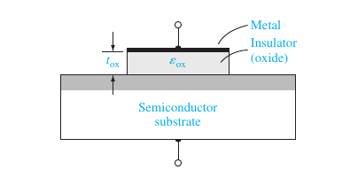
MOSCAP #
- Important: Hardware debugging; can trace buggy device ultimately to unexpected transistor behaviour
- Modeling can be used to predict, but it should be simple; avoid excessive variables
- MOSFET is easy to fabricate: Si is abundant and Si/SiO2 is close to an ideal interface
- Used in digital design as a voltage-controlled switch (gate voltage decides whether source touches drain)
Oxide layer #
- Oxide layer provides insulation (huge band gap) between metal-semiconductor, i.e. the capacitor gap
- It has a built-in electric field \[E = \frac{|W_1-W_2|}{qd}\] which causes band bending towards the side with greater work function, i.e.
- \[C’_{ox} = \frac{\epsilon_{ox}}{T_{ox}} \text{ where } T_{ox}: \text{dielectric thickness} \]
- Prime indicates capacitance (or charge) per unit area.
Accumulation mode #
- On applying a negative voltage, electrons accumulate on the metal, and holes (majority carriers) from the bulk accumulate on the oxide–semiconductor interface which corresponds to the positive charge on the bottom “plate” of the MOS capacitor.
- Flat band: Intrinsic band bending due to \(\phi_{MS}\) needs to be undone before we can enter accumulation mode, as the Fermi level is closer to the intrinsic Fermi level than we want
- Thus, we need to apply a positive voltage on the semiconductor side and negative on metal side:\[ |-V| > |\phi_{MS}| \]
- p-type substrate: accumulation on the negative side of C-V curve
- High or low frequency, accumulation region remains same, change happens in inversion region
Depletion mode #
\[V = \phi_{MS} + \phi_F\]
- \( V_{GS} = \phi_{MS}\) will undo band bending (flat band) and to bring back \(E_F = E_i\) we need to apply an additional voltage \(\phi_F = E_F - E_i\)
- \[\phi_F = V_T \ln{\frac{N_a}{n_i}}\]
Inversion mode #
- By applying a sufficiently large positive gate voltage, we have inverted the surface of the semiconductor from a p-type to an n-type semiconductor. We have created an inversion layer of electrons at the oxide–semiconductor interface (whose electron concentration = majority hole concentration @ bulk)
- Depletion region still exists along with this inversion layer
Depletion Layer Analysis #
Charge profile #
\[\rho = \begin{cases} 0 & x > x_d \\ -qN_A & 0 \le x \le x_d \end{cases}\]
E-field profile #
- Linear with negative slope in sc and \(\mathcal{E}_{max}\) @ surface, constant in oxide, and zero in metal
- As displacement field vector is constant, \[\epsilon_{ox}\mathcal{E}_{ox} = \epsilon_{Si}\mathcal{E}_{max} = Q_d\] i.e. field in oxide is greater than \(\mathcal{E}_{max}\)
Potential profile #
- quadratic in sc, linear in oxide, constant in metal
- \[V_{ox} = \frac{E_{ox}T}{\epsilon_{ox}}T_{ox} = \frac{\epsilon_{Si}E_{Si}}{C_{ox}} = \frac{Q_d}{C_{ox}}\]
- \[Q_d = qN_ax_d\]
- \[V_S = \frac{1}{2}E_sx_d \text{(from graph)}= \frac{1}{2}\frac{qN_ax_d}{\epsilon_{si}}x_d\]
- Gate voltage \[V_G = V_{ox}+V_S = \frac{qN_Ax_d}{C_{ox}} + \frac{qN_Ax_d^2}{2\epsilon_{Si}}\]
Thickness #
- \[x_d = \sqrt{\frac{2\epsilon_S\phi_s}{qN_A}}\] where \(\phi_s: \text{surface potential}\)
- \[C’_{dep} = \frac{\epsilon_s}{x_{d(max)}} \]
- The maximum space charge width, \(x_{d(max)}\), at this inversion transition point can be calculated from the above equation by setting \(\phi_s = 2\phi_F\), since at inversion the potential drop at surface is the negative of the potential drop in the bulk which is \(\phi_F\). This happens at threshold voltage \[V_T = V_S+V_{ox} = 2\phi_F+\frac{qN_Ax_{d{max}}}{C_{ox}}\]
- Beyond \(V_T\), the depletion width does not change much, as all the extra voltage after that is dropped across the oxide, due to the inversion layer’s high density of charge. (\(V_S\): constant)
CV characteristics #
- Useful in debugging and understanding MOSFET properties
- Time-varying signal required, so we apply a small ac voltage with dc.
Accumulation #
\[C = C_{ox} = \frac{dQ}{dV} = \frac{\epsilon_{ox}}{t_{ox}}\]
Depletion #
- \(x_d = f(V_G)\), charge in depletion layer responds to applied voltage
- This adds a \(C_s\) in series along with \(C_{ox}\)
- \[C_{eff} = \frac{C_sC_{ox}}{C_s+C_{ox}}\]
Inversion #
-
We don’t know if the electrons depletion region or the inversion layer are responding to the applied voltage.
- This depends on the frequency of applied signal. When inversion charge responds, frequency of change of voltage is slow enough that it responds.
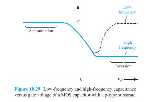
- Low freq (1-10 Hz) \(\rightarrow C_{ox}\)
- High freq (~100 kHz) \(\rightarrow C_{dep}\)
-
Freq vs Temp
- Low Temp (25°C): High freq
- High Temp (150°C): Low freq due to higher generation rate, i.e. charge appears to be available for longer duration
MOSFET #
- It has two pn-junctions. Each pn-junction is a diode.
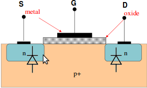
- We use the varcap for controlling (via \(V_G\)) the conductivity of the surface. MOSFET is a surface device.
- When \(V_G>0 \text{ and } V_{GS} > V_T\), i.e. inversion, n+-n-n+ structure which is conducting, so \(I_{DS}\uparrow\) for a given \(V_{DS}\)
- \(V_G<0, I_{DS} \text{ is low}\)
Working Principle #
- Metal work function is such that \(@ V_G = 0\), moscap in depletion.
- Thus, the depletion region of the MOSCAP does not allow any current i.e. \(I_{DS} = 0\), even if \(V_{DS}\) is increased from zero, which only increases the depletion width of drain (more reverse-bias)
- It also blocks current from going to the body, we only want current from source to drain, if any
- Thus, the depletion region of the MOSCAP does not allow any current i.e. \(I_{DS} = 0\), even if \(V_{DS}\) is increased from zero, which only increases the depletion width of drain (more reverse-bias)
- At some \(V_D, Q_{inv} = 0\) at the drain, known as pinchoff.
- Condition: \(V_{GD} = V_T\) i.e. \(V_{D(sat)} = V_G - V_T\)
- On increasing it further, i.e. \(V_D > V_{D(sat)}\), pinch off point moves inwards
Regions #
Can think of it as a black box with modes to model it without pondering the physics
Cutoff #
\(|V_{GS}| < |V_T| \rightarrow I_{DS} = 0\)
- nMOS: \(V_{GS} < V_{T_n}\)
- pMOS: \(V_{GS} > V_{T_p}, V_{T_p} < 0\)
- Until \(|V_{GS}| > |V_T|\), the mos is off and can’t be in any other region. Can be used as a switch
Linear #
Close to \(V_{DS} = 0 \rightarrow I_{DS} \propto V_{DS}\), behaves like a resistor
Triode #
\(V_{DS} < V_{D(sat)}\), difference from linear region is that \(I_D\) is a function of both \(V_{DS}, V_{GS}\)
Saturation #
When \(V_D > V_{D(sat)}, I_{DS} = I_{D(sat)} = f(V_{GS})\), i.e. current is saturated
- current source
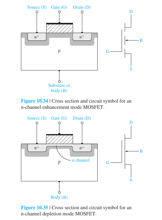
Types #
- nMOS and pMOS
- Enhancement and depletion mode MOSFETS
- Enhancement: Normally off, apply a \(V_G\) to reduce the resistance and turn it on
- Depletion: Normally on, apply a \(V_G\) to shut it off.
Diode Connected MOSFET #
Drain and Gate short-circuited, making \(V_{DS} = V_{GS}\) so \(V_{DS} > \overbrace{V_{D(sat)}}^{V_{GS}-V_T}\) always. So it is either turned off or in saturation (square-law device)
Modeling #
- \(Q_i = -C_{ox}(V_{GS} - V_T(x))\)
- \(V_T = \phi_{ms} + (2\phi_F+V(x))+V_{ox}\)
- \(V_{ox} = Q_i/C_{ox}\)
- \(Q_i = \sqrt{2\epsilon_SN_Aq(2\phi_F+V(x))}\)
- Modeling the mos as a series of resistors, \(dV = I_D dR\)
- \(dR = \frac{dx}{\underbrace{\sigma}_{\propto \ Q_I(x)} W}\)
- \(\boxed{I_Ddx = \mu Q_I(x)dV}\)
- \(V_{DS} > 0\) (small), then \(V(x)\) becomes 0
- \[I_{DS} = \mu C_{ox} \frac{W}{L}(V_{GS}-V_T)\]
Transfer characteristics #
\(g_m = \frac{\partial I_{DS}}{\partial V_{GS}}\) \[g_m|_{sat} = \frac{W}{L} \mu_{neff}C_{ox}(V_{GS}-V_T)\]
Effect of substrate bias #
- Normally \(V_B=0, V_S=0\) and vary \(V_{GS}, V_{DS}\)
- But if \(V_B\) is increased, \(V_{GB}\downarrow\), and we need to apply a higher gate voltage to get same surface potential.
- \(V_T = V_{FB}+\frac{\sqrt{2\epsilon_SqN_A(2\phi_F+V_{BS})}}{C_{ox}}+2\phi_F\) [higher voltage needed, thus addition]
- \(\Delta V_T = V_T - V_{T_0} = \frac{1}{C_{ox}}\sqrt{2\epsilon_SqN_A}[\sqrt{2\phi_F+V_{BS}}-\sqrt{2\phi_F}] \approx \frac{1}{C_{ox}}\sqrt{2\epsilon_SqN_A}\sqrt{V_{BS}} = \underbrace{\gamma}_{\text{Body factor}}\sqrt{V_{BS}}\) [assuming \(V_{BS} \ll 2\phi_F\)]
- Popular technique in the past to change threshold voltage, no longer used
- \(\Delta V_T = V_T - V_{T_0} = \frac{1}{C_{ox}}\sqrt{2\epsilon_SqN_A}[\sqrt{2\phi_F+V_{BS}}-\sqrt{2\phi_F}] \approx \frac{1}{C_{ox}}\sqrt{2\epsilon_SqN_A}\sqrt{V_{BS}} = \underbrace{\gamma}_{\text{Body factor}}\sqrt{V_{BS}}\) [assuming \(V_{BS} \ll 2\phi_F\)]
- \(V_T = V_{FB}+\frac{\sqrt{2\epsilon_SqN_A(2\phi_F+V_{BS})}}{C_{ox}}+2\phi_F\) [higher voltage needed, thus addition]
Non-ideal MOSFET #
Real Threshold Voltage #
\[ V_T = \phi_{MS}+2\phi_F+\frac{|Q_d|}{C_{ox}}\]
- In W-Si, \(\phi_{MS} > 0\) (band bending causes accumulation) whereas \(\phi_{MS} < 0\) in Al-Si (band-bending causes inversion)
- Changing metal contact from Al to W shifts C-V graph right by \(\Delta V_T\)
Fixed charge #
- Fixed charge from manufacturing @ Ox/Si interface (Dangling bonds)
- This reduces \(V_T\) by \[\Delta V_T = \frac{-Q_F}{C_{ox}}\] (C-V graph: parallel shift to left)
Channel length modulation #
- At some point in saturation, in pinchoff: as we increase \(V_D\), \(\Delta L\) increases which reduces effective channel length from \(L \text{ to } L-\Delta L\)
- We can model this non-ideality using the channel length modulation factor \(\lambda\): \[I_{DS} = \frac{1}{2}\mu_{neff}C_{ox}\frac{W}{L}(V_{GS}-V_T)^2(1+\lambda V_{DS})\]
- \(\frac{\partial I_{DS}}{\partial V_{DS}} = \lambda I_{DSAT}\)
- Thus, resistance \[r_0 = \frac{1}{\lambda I_{DSAT}}\]
Mobility of carriers in MOSFETS #
- Smaller in a real MOS than in regular semiconductor, as the oxide surface is rough, and more interaction (collision) occurs
- Model it as \[\mu(V_{GS}) = \frac{\mu_{eff_0}}{1+\theta(V_{GS}-V_T)}\]
- \(I_{DS}|_{real} \propto (V_{GS}-V_T)^\alpha \) [Power law model]
High field effects #
- Reducing channel width \(L\) increases electric field. But eventually, drift velocity saturates (saturated velocity regime), and there is no benefit to reducing L.
- \[I_{DS} = \underbrace{WC_{ox}(V_G-V_T)}_{\text{total charge of channel}}v_{sat}\]
BJT #
- Older technology, still used in RF/high frequency applications
- If we manage to inject holes into the depletion region of a pn-junction in reverse bias, the high electric field will cause high carrier velocity, i.e. high current. [similiar to avalanche breakdown]
- A p+-n junction in forward bias can act as a hole injector (heavily doped p injects holes into n-side)
- So, a BJT can be constructed from the two junctions of a P(+)NP setup.
- Holes are emitted from P+ (emitter) into the central n-region.The high electric field of the second junction (NP) in reverse bias forces them into the collector, not giving a chance to the base to snatch them.
- So, \(I_E \sim I_C\) and \(I_B = I_E-I_C\)
- If base width (W: critical param) is narrow, it can be modelled as two diodes
- Two diodes talking through the base
Advantages over MOSFET #
- Threshold voltage of device only depends on band gap of sc, better control during manufacturing; however, difficult to vary it
- High transconductance, MOSFETs have caught up though
- Outputs high current per unit area i.e. high current density supported. Used a lot in lasers, LEDs (optical devices)
- Works the same with III-V semiconductors as with silicon
Drawbacks #
- Lower power design unsupported
- Minority carrier device: charge storage worries
- Simpler to make a MOSFET. Manufacturing BJT is more complex
Regions #
| Region | EB | CB |
|---|---|---|
| Active | F | R |
| Saturation | F | F |
| Cutoff | R | R |
| Inverted | R | F |
Active #
- \(I_C \approx I_{E_p}\)
- \(I_B \approx I_{E_n}+I_{C_n}+I_{\text{hole recombination}}\)
- Current (\(I_B\)) Controlled Current Source