Digital Design
— HimanishNumber Systems #
\[N = a_n\cdots a_0 . a_{-1}\cdots a_{-m}\]
DEC: \(a_j \in \{0..9\}\)BIN: \(a_j \in \{0, 1\},\ (N)_{10} = \sum_k a_k\cdot 2^k \ \ | \ (N)_2 = a_n\cdots a_0 . a_{-1}\cdots a_{-m} \)OCT: \(a_j \in \{0..7\}\)HEX: \(a_j \in \{0..9, A..F\}\)- In general, \(\left(a_n\cdots a_0 . a_{-1}\cdots a_{-m}\right)_r = (\sum_k a_k \cdot r^k)_{10}\)
Conversion #
DEC to base-k #
- Divide by \(k\) to get \(a_0\) as remainder and quotient \(q_0\)
- Divide \(q_0\) by \(k\) to get \(a_1\) as remainder and quotient \(q_1\)
- Repeat till zero quotient.
- If fractional part present, multiply that by \(k\) to get \(a_{-1}\) as integral part and fractional part \(f_0\)
- Multiply \(f_0\) by \(k\) to get \(a_{-2}\) as integral part and fractional part \(f_1\).
- Repeat till a pattern emerges or sufficient accuracy reached.
Complements #
\[ r\text{’s complement} = r^n - N = \overbrace{(r^n-1) - N}^{(r-1)\text{’s complement}} + 1 \]
- In base \(r\), \((r-1)\)’s complement can be found by subtracting each digit from \((r-1)\) e.g. in base 10, subtract 256 from 999 and in base 2, just swap 1’s and 0’s
Signed Binary Numbers #
| System | Range |
|---|---|
| Unsigned | \([0, 2^N-1]\) |
| Sign/Magnitude | \([–2^{N–1} + 1, 2^{N–1} – 1]\) |
| Two’s Complement | \( [–2^{N–1}, 2^{N–1} – 1]\) |
Sign/magnitude #
- An N-bit
sign/magnitudenumber uses the most significant bit as the sign and the remaining N−1 bits as the magnitude. - ordinary binary addition does not work for sign/magnitude numbers.
- Both +0 and −0 exist.
2’s complement #
- Zero has a single representation, and ordinary addition works.
- Subtraction is performed by taking the two’s complement of the second number, then adding
- Hence, a number’s sign is reversed by taking its 2’s complement
- when adding N-bit numbers, the carry out of the Nth bit (i.e., the (N + 1)th result bit) is discarded.
- Unlike unsigned numbers, a carry out of the most significant column does not indicate overflow. Instead, overflow occurs if the two numbers being added have the same sign bit and the result has the opposite sign bit.
- When a two’s complement number is extended to more bits, the sign bit must be copied into the most significant bit positions. This process is called sign extension. For example, the numbers 3 and −3 are written as 4-bit two’s complement numbers 0011 and 1101, respectively. They are sign-extended to seven bits by copying the sign bit into the three new upper bits to form 0000011 and 1111101, respectively.
Logic #
Logic Gates #
XOR #
- Output of \(A \oplus B\) is
1if A or B, but not both, are1. - An N-input XOR gate is sometimes called a parity gate and produces a
1output if an odd number of inputs are1.
NAND #
Output is 1 unless both inputs are 1.
NOR #
Output is 1 if neither input is 1.
Boolean equations #
Terminology #
- The complement of a variable A is its inverse A’. The variable or its complement is called a literal.
- The
ANDof one or more literals is called a product or animplicant. A minterm is a product involving all of the inputs to the function. - Similarly, the OR of one or more literals is called a sum. A maxterm is a sum involving all of the inputs to the function.
SOP form #
- A Boolean equation for any truth table can be found by summing each of the minterms for which the output, Y, is
1 - The sum-of-products canonical (or standard) form can also be written in sigma notation, e.g. the function \(F(A, B) = m_1+m_3 = \sum(1, 3)\)
- To express a Boolean function in its sum‐of‐minterms form, first expand the expression into a sum of AND terms. Each term is then inspected to see if it contains all the variables. If it misses one or more variables, it is ANDed with an expression such as \(x + x’\), where x is one of the missing variables.
POS form #
- Product of maxterms for which output is
0 - To express a Boolean function as a product of maxterms, it must first be brought into a form of OR terms. This may be done by using the distributive law, \(x + yz = (x + y)(x + z)\). Then any missing variable x in each OR term is ORed with \(xx’\)
Boolean algebra #
- Axioms and theorems of Boolean algebra obey the principle of duality. If the symbols 0 and 1 and the operators • (AND) and + (OR) are interchanged, the statement will still be correct.
Boolean theorems of several variables #
| Theorem | Dual | Name |
|---|---|---|
| ΒC + ΒD = Β(C + D) | (B + C)(B + D) = B + CD | Distributivity |
| Β(Β + C) = Β | B + BC = B | Covering |
| ΒC + BC’ = Β | (B + C)(B + C’) = B | Combining |
| ΒC + B’D + CD = BC + B’D | (B + C)(B’ + D)(C + D) = (B + C)(B’ + D) | Consensus |
Bubble pushing #
- Pushing bubbles backward (from the output) or forward (from the inputs) changes the body of the gate from AND to OR or vice versa.
- Pushing a bubble from the output back to the inputs puts bubbles on all gate inputs.
- Pushing bubbles on all gate inputs forward toward the output puts a bubble on the output.
Gate-level minimisation #
Selecting the best multilevel implementation of a specific logic function is not a simple process. Moreover, “best” has many meanings: fewest gates, fastest, shortest design time, least cost, least power consumption. For example, we have been using ANDs and ORs, but in CMOS, NANDs and NORs are more efficient.
Bubble pushing for CMOS Logic #
- Begin at the output of the circuit and work toward the inputs.
- Push any bubbles on the final output back toward the inputs so that you can read an equation in terms of the output (for example, Y) instead of the complement of the output (Y’).
- Working backward, draw each gate in a form so that bubbles cancel. If the current gate has an input bubble, draw the preceding gate with an output bubble. If the current gate does not have an input bubble, draw the preceding gate without an output bubble.
Logic Minimization with K-Maps #
An implicant is called a prime implicant if it cannot be combined with any other implicants in the equation to form a new implicant with fewer literals. The implicants in a minimal equation must all be prime implicants.
Digital Building Blocks #
Addition #
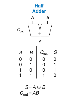
Half adder #
Full adder #
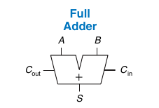 \[S = A \oplus B \oplus C_{in}\]
\[C_{out}=AB+AC_{in}+BC_{in}\]
\[S = A \oplus B \oplus C_{in}\]
\[C_{out}=AB+AC_{in}+BC_{in}\]
Carry Propogate Adders (CPAs) #
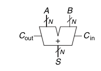 There are three common CPA implementations: ripple-carry adders, carry-lookahead adders, prefix adders.
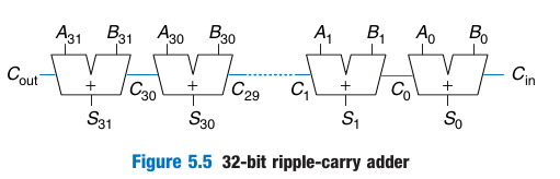
Ripple-Carry Adder #
Simplest way; chain together N full adders. \(C_{out}\) of one stage acts as \(C_{in}\) for next stage. Disadvantage: Slow when N large. The carry ripples through the carry chain.
Carry-Lookahead Adder (CLA) #
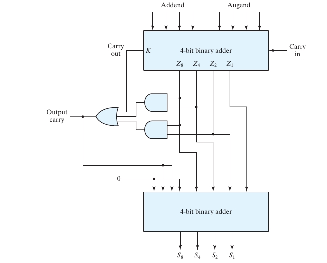
BCD Adder #
- The adder will form the sum in binary and produce a result that ranges from 0 through 19. These binary numbers are listed in Table 4.5 and are labeled by symbols \(K, Z_8, Z_4, Z_2, and Z_1\). K is the carry, and the subscripts under the letter Z represent the weights 8, 4, 2, and 1 that can be assigned to the four bits in the BCD code.
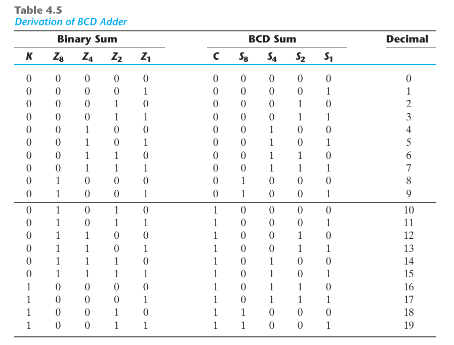
- When the binary sum is equal to or less than 1001, the corresponding BCD number is identical, and therefore no conversion is needed. When the binary sum is greater than 1001, we obtain an invalid BCD representation. The addition of binary 6 to the binary sum converts it to the correct BCD representation and also produces an output carry as required.
- The condition for a correction and an output carry can be expressed by the Boolean function \(C = K + Z_8Z_4 + Z_8Z_2\)
- A decimal parallel adder that adds n decimal digits needs n BCD adder stages.
Subtraction #
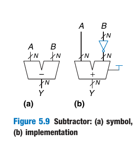 To compute Y = A − B, first create the two’s complement of B: Invert
the bits of B to obtain B’ and add 1 to get −B = B’ + 1. Add this quantity to
A to get Y = A + B + 1 =
To compute Y = A − B, first create the two’s complement of B: Invert
the bits of B to obtain B’ and add 1 to get −B = B’ + 1. Add this quantity to
A to get Y = A + B + 1 = A − B. This sum can be performed with a single
CPA by adding A + B with \(C_{in} = 1\).
Adder-Subtractor #
The input carry \(C_0\) must be equal to 1 when subtraction is performed. The addition and subtraction operations can be combined into one circuit with one common binary adder by including an exclusive-OR gate with each full adder:
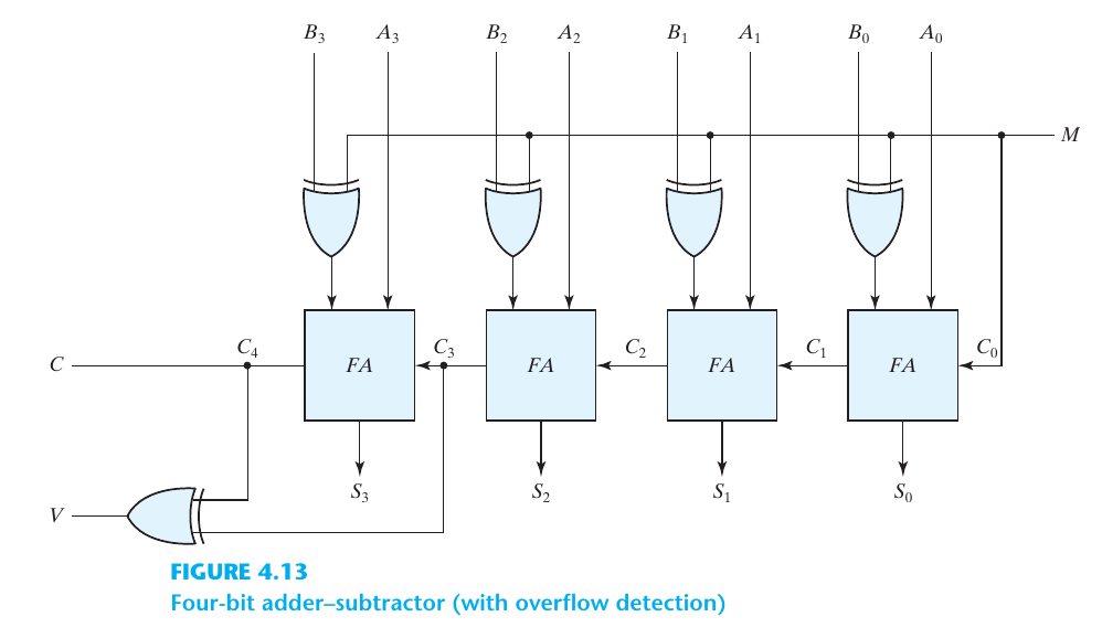 The mode input M controls the operation.
When M = 0, the circuit is an adder, and when M = 1, the circuit becomes a subtractor. It is worth noting that binary numbers in the signed-complement system are added and subtracted by the same basic addition and subtraction rules as are unsigned num- bers. Therefore, computers need only one common hardware circuit to handle both types of arithmetic. The user or programmer must interpret the results of such addition or subtraction differently, depending on whether it is assumed that the numbers are signed or unsigned.
Multiplication #
For J multiplier bits and K multiplicand bits, we need \(J \times K\) AND gates and (J - 1) K-bit adders to produce a product of (J + K) bits.
Magnitude Comparator #
- The equality function \(\ \ x_i = A_iB_i+A_i’B_i’ \quad | \ i = 0..n-1\)
- \((A = B) = x_3x_2x_1x_0 \ (4-\text{bit}) \)
- \((A > B) = A_3B_3’+x_3A_2B_2’+x_3x_2A_1B_1’+x_3x_2x_1A_0B_0’\)
- \((A < B) = A_3’B_3+x_3A_2’B_2+x_3x_2A_1’B_1+x_3x_2x_1A_0’B_0\)
Combinational Logic #
Decoder #
- N inputs and \(2^N\) outputs. If input has unused combinations, may have fewer than \(2^N\) outputs.
- Asserts exactly one of its outputs depending on the input combination.
- Can be used to build logic functions. Because each output of a decoder represents a single minterm, the function is built as the OR of all the minterms in the function.
Enable #
- A decoder with enable input can function as a demultiplexer—a circuit that receives information from a single line and directs it to one of \(2^n\) possible output lines.
- Decoders with enable inputs can be connected together to form a larger decoder circuit
- In general, enable inputs are a convenient feature for interconnecting two or more standard components for the purpose of combining them into a similar function with more inputs and outputs.
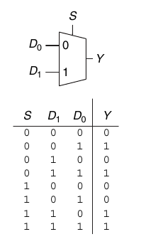
Multiplexer #
2:1 Mux #
Two data inputs \(D_0\) and \(D_1\), a select input S, and one output Y. The multiplexer chooses between the two data inputs based on the select.
- If S = 0, Y = \(D_0\), and if S = 1, Y = \(D_1\). S is also called a control signal because it controls what the multiplexer does.
- It can be built from sum-of-products logic or tristate buffers.
Wider Muxes #
A 4:1 multiplexer has four data inputs and one output, two select signals are needed.
- Implementation
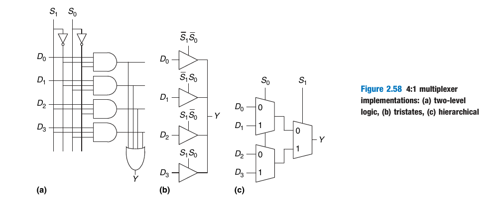
Comparison with Decoder #
- The AND gates and inverters in the multiplexer resemble a decoder circuit, and indeed, they decode the selection input lines. In general, a \(2^n\)-to-1-line multiplexer is constructed from an n-to-\(2^n\) decoder by adding \(2^n\) input lines to it, one to each AND gate.
- As in decoders, multiplexers may have an enable input to control the operation of the unit. When the enable input is in the inactive state, the outputs are disabled.
n-variable function using n-1 selection input multiplexer #
- The first n - 1 variables of the function are connected to the selection inputs of the multiplexer. The remaining variable of the function is used for the data inputs.
- For each combination of the selection variables, we evaluate the output as a function of the last variable \(z\). This function can be 0, 1, \(z\), or \(z’\). These values are then applied to the data inputs in the proper order.
Synchronous Sequential Logic #
The outputs of sequential logic depend on both current and prior input values. Hence, sequential logic has memory. Sequential logic might explicitly remember certain previous inputs, or it might distill the prior inputs into a smaller amount of information called the state of the system. The state of a digital sequential circuit is a set of bits called state variables that contain all the information about the past necessary to explain the future behavior of the circuit.
Cross-Coupled Inverter #
- The fundamental building block of memory is a bistable element, an element with two stable states.
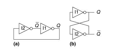
- Because the cross-coupled inverters have two stable states, Q=0 and Q=1, the circuit is said to be bistable. A subtle point is that the circuit has a third possible state with both outputs approximately halfway between 0 and 1. This is called a metastable state.
- Just as Y is commonly used for the output of combinational logic, Q is commonly used for the output of sequential logic.
- The state of the cross-coupled inverters is contained in one binary state variable, Q. The circuit does have another node, Q’, but Q’ does not contain any additional information because if Q is known, Q’ is also known.
- They are not practical because the user has no inputs to control the state.
Latches #
SR Latch #
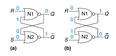 (NOR gates are used to build active high SR latches and NAND gates to build active low SR latches)
- The inputs S and R stand for Set and Reset. To set a bit means to make it TRUE. To reset a bit means to make it FALSE.
- The outputs, Q and Q’, are normally complementary. When R is asserted, Q is reset to 0 and Q’ does the opposite. When S is asserted, Q is set to 1 and Q’ does the opposite. When neither input is asserted, Q remembers its old value, \(Q_{prev}\).
- Asserting both S and R simultaneously doesn’t make much sense because it means the latch should be set and reset at the same time, which is impossible. The poor confused circuit responds by making both outputs 0.
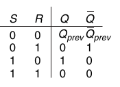
- Unlike the cross-coupled inverter, the state can be controlled through the S and R inputs.
- SR NAND latch is an inverted version of SR NOR latch.
D Latch #
The SR latch is awkward because it behaves strangely when both S and R are simultaneously asserted. Moreover, the S and R inputs conflate the issues of what and when. Asserting one of the inputs determines not only what the state should be but also when it should change.
- The D latch has two inputs. The data input, D, controls what the next state should be. The enable input, En, controls when the state should change.
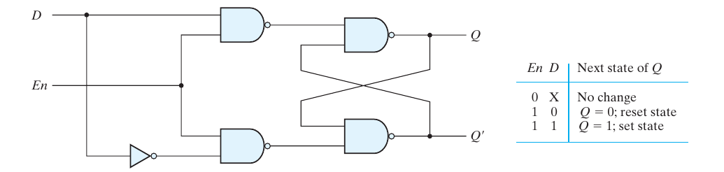
- When En = 1, the latch is transparent. The data at D flows through to Q as if the latch were just a buffer. When En = 0, the latch is opaque. It blocks the new data from flowing through to Q, and Q retains the old value. Hence, the D latch is sometimes called a transparent latch or a level-sensitive latch.
Flip-flops #
JK #
\[D = JQ’ + K’Q\]
State Diagrams #
- It is important to remember that the bit value listed for the output along the directed line occurs during the present state and with the indicated input, and has nothing to do with the transition to the next state.